Recommended problems i Semiconductor Devices and fabrication, TNE058, HT 2011
Examiner Amir Baranzahi
No. 1:
Problems. 1.24 (Hint ΔE in the problem is one single stat and not an energy interval) ,
Problem2: A GaAs sample, n-type, 1017cm-3 , calculate and plot EF for RT and 400K, assume all dopants are ionized
2.16 Hint read page 38 for Joice-Dixon approximation)
Problem 6 In Cumulative Problems Chap. 1-2.
problem 9 in Cumulative Problems Chap. 1-2
No. 2:
Problem 3.7, 3.14, and problems 3 and 4 under Cumulative Problems Chap. 1-3.
Problem. 5:
n-type Si with Nd= 5*1015 cm-3, is illuminated
such that 1021 cm-3s-1 e-h-pair is generated in
the whole volume.![]() for this
sample. Calculate the separation of quasi-fermi levels,
for this
sample. Calculate the separation of quasi-fermi levels,
![]() , draw an
energy band diagram similar to Fig. 3.8c, T= 300K
, draw an
energy band diagram similar to Fig. 3.8c, T= 300K

Problem6:
A GaAs sample with Nd= 1*1015 cm-3 illuminated
as in the drawing above, Illumination is such that 1021 cm-3s-1
e-h-pairs are generated in the part of sample that is not screened (see Fig.). At
what distances, x, the electron and hole concentrations decreased to 50%? Note
the origin is at the beginning of the screened part of the sample.
![]() , T=300K.
, T=300K.
No. 3:
Problems: Jaspirit Singh: 5.4, 5.5, 5.7, 5.9, 5.16, 5.23, 5.27
No. 4:
Problems from Jaspirit Singh: 5.26 (note that the values in graph in formelsamling are not sufficient for the highly doped p-n-junction here), 5.28, 6.3, 6.11, IV.1, IV.2
IV.1 Platinum-silicon carbide, Pt-SiC*, contact is formed, work
![]() =
5,65 eV, Nd = 1016 cm-3,
=
5,65 eV, Nd = 1016 cm-3,![]() = 3,5 eV, Eg,SiC= 3,26 eV , T=300K,
= 3,5 eV, Eg,SiC= 3,26 eV , T=300K,
![]()
a) Calculate the built-in potential Vo (6P)?
b) Is it possible to get Pt-SiC contact ohmic? If not suggest an ohmic metal-SiC contact? Motivate your answers. (6P)
IV.2 You wish to have a simple and cheap voltage stab which gives you a 15V stable constant voltage. (Your power generator generates a voltage between 15 and 18 V).You call Elfa and they tell you advice you to use breakdown diodes, what kind of breakdown mechanism is they are talking about? Why? (2P)
No. 5:
Problems from Jasprit Singh:
9.5: use data from Fig. 9.5, Turn on voltage=threshold voltage, oxide charge is given as density (multiply with q to get the charge)
9.7: Use data in Fig. 9.5
9.14:
9.15: Note electrons’ and holes’ mobilities are for channel and not for the bulk.
9.17:
9.20:
No. 6:
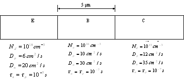
BJT1: npn-BJT in Si as above
Emitter and collector lengths are much longer than diffusion lengths for electrons and holes.
A= 0,01 cm2, T= 300K.
Calculate
and plot minority carrier profiles,![]() when
EB junction is forward biased VEB= 0,5 V and BC junction is reverse
biased with VBC= -5.
when
EB junction is forward biased VEB= 0,5 V and BC junction is reverse
biased with VBC= -5.
BJT 2:
Calculate amplification factor,
![]() ,
in problem BJT1 above.
,
in problem BJT1 above.
BJT3: Bandgaps narrowing: The bandgap of a semiconductor decreases somewhat with the temperature and with the doping. Eqvation 7.111 gives the bandgap shrinkage for silicon. Use this relation and solve problem 7.30 in Singh (please read the whole text and consider the application range and limitation of the equation).
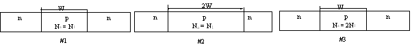
BJT4: Three n-p-n transistors (above) are identical except that transistor #2 has a base region twice as long as transistor #1, and transistor #3 has a base region doped twice as heavily as transistor #1. All other dopings and lengths are identical for the three transistors. Which transistors have the largest value of each parameter listed below?
Give clear mathematical reason for each of your answers.
a) Emitter injection efficiency
b) Base transport factor
c) Punch through voltage
d) Collector junction capacitance with VBC= -10 V.
e) Common emitter current gain.
BJT5: Singh chap 7, Design problem 4
* SiC is a semiconductor that functions at much higher temperature than Si. There are different crystal structures for SiC, the values here are for n-type, 4H SiC.